 Loading image. Please wait
Panel fabrication facility which Gratings Inc have setup in Indonesia in partnership with AZET


Panel fabrication facility which Gratings Inc have setup in Indonesia in partnership with AZET
Panel fabrication facility which Gratings Inc have setup in Indonesia in partnership with AZET
Panel fabrication facility which Gratings Inc have setup in Indonesia in partnership with AZET
Controllable diameter (~ 4 nm) and separation (12 nm) Au nanospheres in SiO2 nanowires
High aspect ratio silicon nanostructures for field emission device applications
Defect-free Ge heteroepitaxial growth of Ge on Si nanostructures
Panel fabrication facility which Gratings Inc have setup in Indonesia in partnership with AZET
A typical solar cell
An electrical model for solar cell
Randomly textured Si structures for solar cell applications
Random reactive ion- etch textured Si structures for solar cell applications
Randomly-textured 6-inch diameter Si solar cell
50 Wp solar panel
150 Wp solar panel
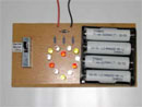
Example of KIT PCB
Example of KIT PCB
Example of KIT PCB
Example of KIT PCB
Panel fabrication facility which Gratings Inc have setup in Indonesia in partnership with AZET